ASML Inks Advanced EUV Lithography Deals With Chip Titans TSMC, Samsung
Barclays analysts called the announcement a “positive” for High NA EUV machines, which are viewed as crucial to ASML’s revenue growth.
Sign up for smart news, insights, and analysis on the biggest financial stories of the day.

The world’s two biggest chipmakers have seen the (ultraviolet) light.
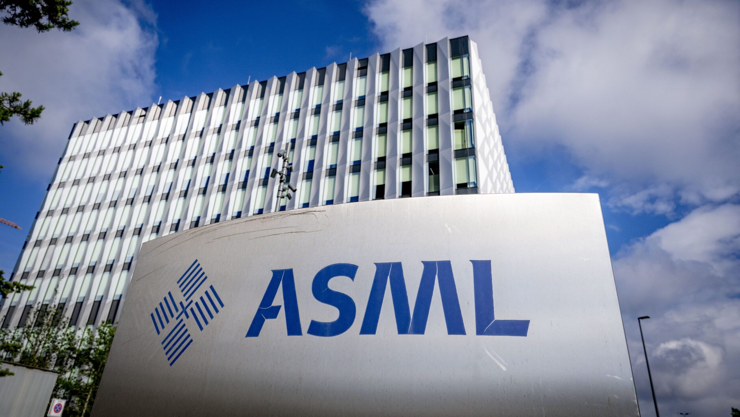
ASML announced Tuesday that Samsung and TSMC agreed to adopt its high-numerical aperture (NA) extreme ultraviolet (EUV) lithography machines to manufacture semiconductors by 2028 and 2030, respectively. If that sounds like too much technical mumbo jumbo, basically it means the already flush company’s photolithography machines could soon print money.
UV Monopoly Protection
The list of companies that can make extreme ultraviolet lithography machines, which are essential to manufacturing the most advanced semiconductors for AI, smartphones and high-end computing, is as follows: ASML. This 100% commercial monopoly has helped lift shares in the Dutch firm 126% in the past year. The more AI demand intensifies, the more demand for AI infrastructure intensifies and the greater the need for ASML’s machines to print the chips needed at new advanced data centers. With Wall Street forecasting trillions of dollars in AI capital expenditures for years, that cycle could run for a while.
ASML, whose machines print microscopic circuit patterns on silicon wafers, debuted its Low NA EUV, now widely used, in 2013. What TSMC and Samsung agreed to adopt on Tuesday is more advanced High NA EUV lithography. It can print smaller features with more precision than Low NA, which means chipmakers can fit more transistors on each semiconductor, increasing their processing power.
Barclays analysts called the announcement a “positive” for High NA EUV machines, viewed as crucial to ASML’s revenue growth. ASML rose 2.91% in New York on Tuesday, and Wall Street sees room for more gains:
- The average target price of $2,414, according to Zacks Investment Research, implies the stock has a 40% upside.
- ASML, Intel, Samsung and TSMC separately agreed Tuesday to double the size of photomasks, the template stencils used to print silicon wafers with UV light, from 6 inches to 12, another step toward faster production.
Poor Imitation: ASML’s stock sank in late July following reports that a state-backed Chinese rival had begun mass-producing ultraviolet lithography tools. At the time, JPMorgan dismissed the selloff as “disproportionate,” noting China has been making lower-end equipment for years “without any impact on ASML’s market share.” Last week, UBS analysts joined in, writing that China is years behind and unlikely to rival ASML’s technology any time soon.
Recent News





-

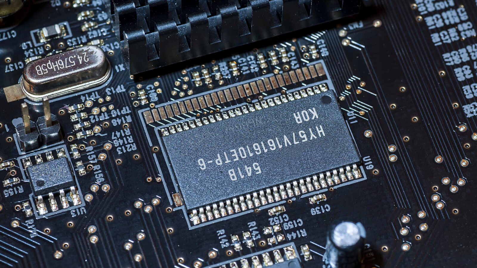
Photo illustration by Connor Lin / The Daily Upside, Photo via Chelsea Blair/Sipa USA/Newscom